|
| LHC BLM threshold modification reports |
Questions of auditors
Can you give details on how the
BLM PCBs have been tested ?
You can find the details on the following file:
Validation_production_BLM_electonic_boards.xls
CFC tests
1. Step: The PCBs have been test for connectivity and short circuits
2. Step: All Cards are put in the test bench to calibrate the 1mA point,
this means all the analogue circuits of the card are tested.
3. Step: All Cards are put in the test bench to adjust the 10pA, this
means all the analogue circuits of the card are tested again.
4. Step: All Cards are put in the test bench for the final test:
Check: FPGA barcode number, FPGA internal number, Board number
Verification of the 10pA
Verification of the 1mA
Check optical link
Check of status: TEMP_1 OK, STATUS TEMP_2, STATUS GOH_1 OK STATE, GOH_2
OK STATE, DAC_OVER_155 OK, DAC_OVERFLOW, POWER SUPPLIES P5V, POWER
SUPPLIES M5V, POWER SUPPLIES P2V5
Scan of the HV levels
Linearity test of the inputs: scan of all channels with 1pA, 10pA, 100pA,
1nA, 10nA, 100nA, 1uA, 10uA, 100uA, 1mA
Check of HV-TEST
Check of the status Level and CRC_ERROR with a negative inout current
Check of GOH-RST
Check of DAC-RST
5. Step: All cards are tested when they have be installed on their final
place, 10pA check and optical link test.
Test of tunnel crates and power supplies and other hardware [excel]
What is the status of the BLM
installation ? Which fraction of BLMs,
electronics, ... are in their final place ?
Status
Can we get input on the
experience from the last 2 weeks of running
the BLMs ? Which type of issues have been discovered ?
We have not a continuous logging over weeks jet, because the concentrator
and the measurement database are under development. We have IP6 and IP5
logging running for the radioactive source measurements.
Source measurements:
1,
2,
3,
4,
5
The main issue is actually to get the acquisition system in a stable
running mode
and on the hardware side
main connector disconnected from the racks, Fiber not plugged
correct, inside the patch boxes and on the cards.
Can you provide us with a global
schematic showing all parts as well
as signal paths, dependencies and power supplies/powering/grounding ?
Some circuit diagrams are shown in the talk of E. Effinger [ppt]
Can you send us details on
the simulation ? We would like to better
understand the full picture starting from the initial protons (beam
loss) up to the current leaving the ionization chamber. How do you
calibrate ?
The whole scheme of how we get the final numbers is presented on page 3 of
Agnieszka's presentation and on page 4 of Mariusz's presentation. The most
complete document describing the simulation chain is study of losses in Triplets,
but this is a special case because of the interaction debris
giving a constant contribution to the losses.
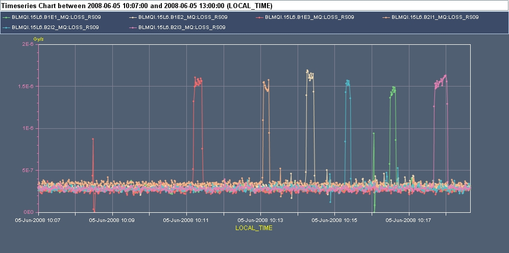
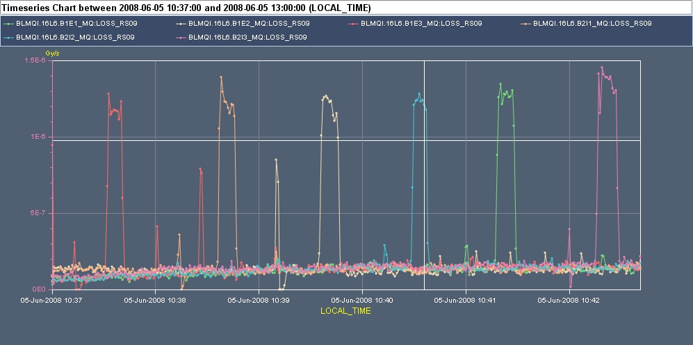
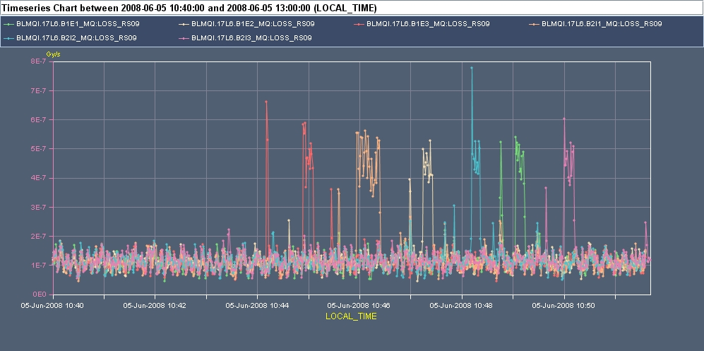
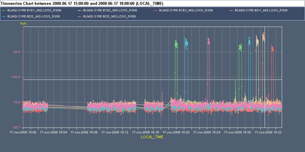
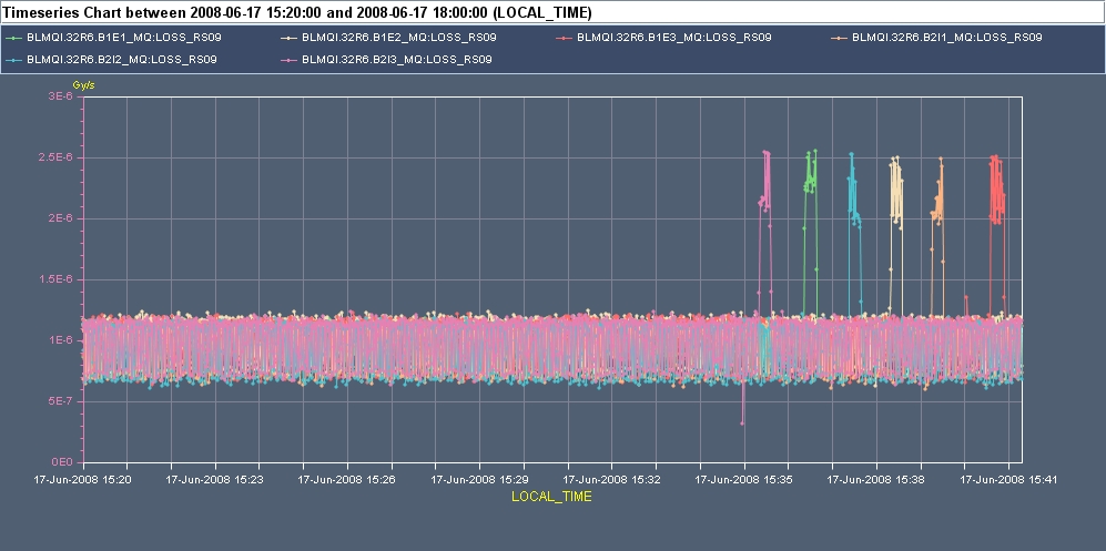
How does a typical signal from a
SPS beam loss / HERA beam loss look
like ? We are in particular interested in the signal vs. time.
Please look at the last 4 slides of Daniel's presentation, which was updated with some
examples of fast losses seen by the Ionization Chambers and the FFTs in case of a
coasting beam. The SEM response to a very fast loss is on the slide 16 compared
to the (saturated) IC with signal filters.
Have you compared such a signal
with the response from e.g. coupling a
pulsed signal into the ionization chamber and propagate this signal
through the full chain ?
Pulsing the system (discharge of a capacitor),
we didn't do such a test but there was the injection test and
we could see signal from the pilot beam. And we pulsed the system in the
SPS beam dump.
How are the HV modulation tests
working ? What is the frequency and
the modulated range ?
You can see 2 slides from the audit
presentation
SLIDE 25: General presentation of the modulation chain
(BLECS->HV_PS->IC->BLECF->BLETC->CPU->BLECS)
SLIDE 45: Presentation of the first results of the modulation and analysis
done in 2007, point 8.
About the
frequency range I would say 10mHz to
100mHz.
As you can see in the simulations, in order to have some signal, I guess the
minimum frequency should be around 10mHz.
The maximum frequency is determined by the offset current at the CFC.
Because the current to frequency input cannot measure negative current, the
modulation contribution to this negative current should not be higher than
the offset current at the CFC (max 100pA in test mode). This constraint
limits the maximum frequency.
A second limitation is the readout of the running sum (1Hz) which limits the
modulation to 100mHz to have at least 10 point per period.
The frequencies foreseen have been chosen also after simulations made by
Erik VERHAGEN: (http://ab-div-bdi-bl-blm.web.cern.ch/ab-div-bdi-bl-blm/Electronics/BLECS_Combiner/BLECS-Simulations/Modulation/SimulModulation.pdf)
It has been shown that if components are changing over time, we could see:
At
30mHz =>
Variation in phase, if the capacitor inside the IC is changing (slide 4).
At
100mHz =>
Variation in gain, if the IC capacitance is changing (slide 5).
After the first tests, it seems that the
modulation amplitude
will be around 5V peak-to-peak at 1600V offset. The maximum modulation
voltage is also linked to the maximum negative input current of the CFC.
Despite you additional
document (the MPSC minutes), we would like also
to deeper understand the entanglement of the master table with the
disable and mask bits. Can you be more specific ?
The Master table contains data in a form which correspond to the image in front end
electronics. It contains maskable / unmaskable and connected/unconnected flags.
Therefore change of any of these flags is equivalent to change of the Master table
and this can be done only by Experts. The only think which can be done by "Operators"
(selected
group) is trimming the threshold values.
This web site is owned by the account czam
Site created by CERN Web Services on Wednesday, 12 March 2003 at 11:30